| CPC H01L 33/58 (2013.01) [H01L 25/0753 (2013.01); H01L 33/46 (2013.01); H01L 33/505 (2013.01); H01L 33/60 (2013.01); H01L 33/62 (2013.01); H01L 2933/0091 (2013.01)] | 14 Claims |

|
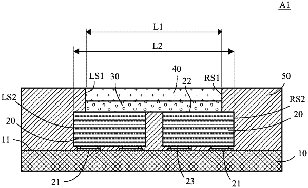
1. A light emitting device, comprising:
a mount substrate;
at least one light emitting element disposed on the mount substrate in a flip-chip manner,
wherein the light emitting element comprises:
a light-transmitting element substrate;
an n-type semiconductor layer disposed on the light-transmitting element substrate;
a light emitting layer disposed on the n-type semiconductor layer;
a p-type semiconductor layer disposed on the light emitting layer, wherein the light emitting layer and the p-type semiconductor layer expose an area of the n-type semiconductor layer;
a first n-electrode disposed on the area of the n-type semiconductor layer;
a first p-electrode disposed on the p-type semiconductor layer;
a first insulating layer disposed on the n-type semiconductor layer so as to insulate the first n-electrode and the first p-electrode from each other;
a second n-electrode disposed on the first n-electrode and the first insulating layer, wherein the second n-electrode has a first area larger than a first joined face between the n-type semiconductor layer and the first n-electrode so that the second n-electrode is electrically connected to the first n-electrode, wherein the second n-electrode is insulated from the first p-electrode by the first insulating layer; and
a second p-electrode disposed on the first p-electrode and the first insulating layer, wherein the second p-electrode has a second area smaller than a third area of the light emitting layer, wherein the second p-electrode is electrically connected to the first p-electrode, wherein the second n-electrode and the second p-electrode have virtually same size and are electrically connected and fixed to the mount substrate;
a first light transparent member that receives incident light emitted from the at least one light emitting element, wherein the first light transparent member is formed of an inorganic substance and an inorganic phosphor, and the first light transparent member has a top surface and a first side surface contiguous to the top surface;
a second light transparent member disposed on the top surface of the first light transparent member, wherein the second light transparent member is only formed of the inorganic substance and contains no the inorganic phosphor, and the second light transparent member has an externally exposed light emission surface and a second side surface contiguous to the externally exposed light emission surface; and
a covering member comprising a light reflective material, and covering at least the first side surface of the first light transparent member and at least the second side surface of the second light transparent member;
wherein the light emitting element is not enclosed by the first light transparent member and not enclosed by the second light transparent member in a plan view from the externally exposed light emission surface side, wherein the first side surface of the first light transparent member and the second side surface of the second light transparent member are located inside a top surface of the light emitting element.
|