| CPC H01L 33/382 (2013.01) [G09G 3/32 (2013.01); H01L 25/0753 (2013.01); H01L 33/40 (2013.01); H01L 33/62 (2013.01); G09G 2300/0426 (2013.01)] | 14 Claims |

|
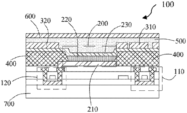
1. A display substrate, comprising:
a plurality of pixel units, at least one pixel unit comprising a light emitting diode and a drive circuit, the light emitting diode comprising a cathode; and
an auxiliary electrode layer comprising at least one auxiliary electrode, wherein the at least one auxiliary electrode is disposed in at least one of the plurality of the pixel units,
wherein the auxiliary electrode is electrically connected with the cathode of the light emitting diode which is located in the same pixel unit as the pixel unit that the auxiliary electrode is located in, and the auxiliary electrode covers at least a portion of the drive circuit in the pixel unit that the auxiliary electrode is located in, the auxiliary electrode is made of an opaque conductive material, so as to block light irradiated at the portion of the drive circuit that is covered by the auxiliary electrode,
wherein the auxiliary electrode layer further comprises auxiliary electrode line, the display substrate comprises a gate line and a data line, and the auxiliary electrode line is for covering the gate line and/or the data line,
wherein the auxiliary electrode line and the auxiliary electrode are independent from each other but being a same conductive material,
wherein no overlap exists between orthographic projections of the auxiliary electrode line and the auxiliary electrode on a substrate of the display substrate, and
wherein the at least one auxiliary electrode comprises a first auxiliary electrode and a second auxiliary electrode, the drive circuit comprises a driving transistor and a switching transistor, and orthographic projections on the drive circuit of the first and second auxiliary electrode are both rectangular in shape and cover the driving transistor and the switching transistor respectively, and
wherein the display substrate further comprises a film encapsulation layer, the auxiliary electrode layer is arranged between the film encapsulation layer and the cathode of the light emitting diode.
|