US 11,688,827 B2
Nanorod semiconductor layer having flat upper surface, micro-LED including the nanorod semiconductor layer, pixel plate including micro-LED, display device including the pixel plate, and electronic devices including the pixel plate
Nakhyun Kim, Yongin-si (KR); Junhee Choi, Seongnam-si (KR); Jinjoo Park, Yongin-si (KR); and Joohun Han, Hwaseong-si (KR)
Assigned to SAMSUNG ELECTRONICS CO., LTD., Suwon-si (KR)
Filed by SAMSUNG ELECTRONICS CO., LTD., Suwon-si (KR)
Filed on Nov. 30, 2020, as Appl. No. 17/106,515.
Claims priority of application No. 10-2020-0073245 (KR), filed on Jun. 16, 2020.
Prior Publication US 2021/0391499 A1, Dec. 16, 2021
Int. Cl. H01L 33/24 (2010.01); H01L 25/16 (2006.01); H01L 29/06 (2006.01); H01L 33/32 (2010.01); H01L 25/075 (2006.01); H01L 33/44 (2010.01)
CPC H01L 33/24 (2013.01) [H01L 25/0753 (2013.01); H01L 25/167 (2013.01); H01L 29/0676 (2013.01); H01L 33/32 (2013.01); H01L 33/44 (2013.01)] 26 Claims
OG exemplary drawing
 
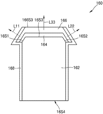
1. A nanorod semiconductor layer comprising:
a main body; and
an upper end connected to an upper part of the main body,
wherein the upper end comprises:
a first inclined surface;
a second inclined surface; and
a flat upper surface between the first inclined surface and the second inclined surface,
wherein a width of the upper end becomes narrower in an upward direction away from the main body.