| CPC H01L 33/06 (2013.01) [H01L 33/0004 (2013.01)] | 19 Claims |

|
1. A light emitting device comprising:
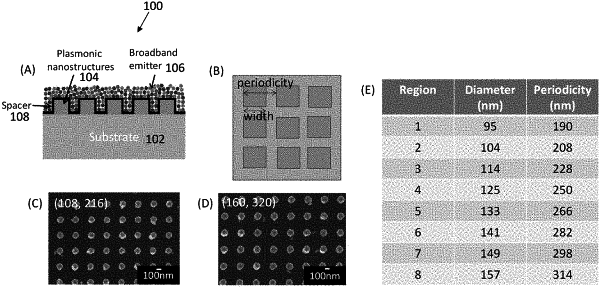
a plasmonic structure comprising a plurality of periodicities, the plurality of periodicities configured to have a corresponding plurality of localized surface plasmon resonances;
a broadband light emitting layer comprising a mixture of a plurality of narrowband emitters, each narrowband emitter having a respective spectral peak, the broadband light emitting layer comprising an emission spectrum substantially overlapping wavelengths of the localized surface plasmon resonances; and
a spacer layer disposed between the plasmonic structure and the broadband light emitting layer;
wherein a color of light emitted by the broadband light emitting layer is tunable by relative intensities of the spectral peaks of the narrowband emitters, the intensities being modified by the localized surface plasmon resonances of the plasmonic structure; and
wherein the plasmonic structure is configured to control a polarization of light emitted by the broadband light emitting layer.
|