| CPC H01L 29/78696 (2013.01) [H01L 21/02532 (2013.01); H01L 21/02636 (2013.01); H01L 21/02664 (2013.01); H01L 21/311 (2013.01); H01L 21/3247 (2013.01); H01L 21/823418 (2013.01); H01L 21/823437 (2013.01); H01L 21/823468 (2013.01); H01L 27/0886 (2013.01); H01L 29/0673 (2013.01); H01L 29/0847 (2013.01); H01L 29/42392 (2013.01); H01L 29/66545 (2013.01); H01L 29/66575 (2013.01); H01L 29/785 (2013.01); H01L 29/7848 (2013.01)] | 20 Claims |
|
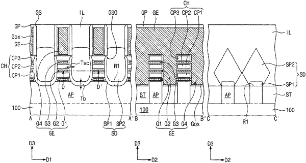
1. A method of fabricating a semiconductor device, the method comprising:
forming a stack structure that includes a plurality of semiconductor patterns and a plurality of sacrificial patterns that are alternately stacked on a semiconductor substrate;
forming a dummy gate electrode that runs across the stack structure and a gate spacer that covers a sidewall of the dummy gate electrode, wherein a portion of the stack structure is exposed outside the gate spacer;
removing the portion of the stack structure exposed outside the gate spacer to form a spacer opening that exposes the stack structure below the dummy gate electrode; and
forming a first source/drain pattern that covers a lateral surface of the stack structure exposed to the spacer opening,
wherein forming the first source/drain pattern includes:
performing a selective epitaxial growth process to form the first source/drain pattern having a first sidewall profile; and
performing a reflow process to change the first sidewall profile of the first source/drain pattern into a second sidewall profile.
|