US 11,688,812 B2
Semiconductor device with treated interfacial layer on silicon germanium
Chih-Yu Chang, New Taipei (TW); Hsiang-Pi Chang, New Taipei (TW); and Zi-Wei Fang, Hsinchu County (TW)
Assigned to TAIWAN SEMICONDUCTOR MANUFACTURING CO., LTD., Hsinchu (TW)
Filed by TAIWAN SEMICONDUCTOR MANUFACTURING CO., LTD., Hsinchu (TW)
Filed on Jun. 3, 2021, as Appl. No. 17/338,426.
Application 17/338,426 is a continuation of application No. 16/853,602, filed on Apr. 20, 2020, granted, now 11,031,508.
Application 16/853,602 is a continuation of application No. 15/919,070, filed on Mar. 12, 2018, granted, now 10,629,749, issued on Apr. 21, 2020.
Claims priority of provisional application 62/593,004, filed on Nov. 30, 2017.
Prior Publication US 2021/0296507 A1, Sep. 23, 2021
This patent is subject to a terminal disclaimer.
Int. Cl. H01L 29/786 (2006.01); H01L 21/28 (2006.01); H01L 21/265 (2006.01); H01L 21/324 (2006.01); H01L 29/66 (2006.01); H01L 29/06 (2006.01); H01L 29/08 (2006.01); H01L 29/10 (2006.01); H01L 29/423 (2006.01); H01L 29/49 (2006.01)
CPC H01L 29/78696 (2013.01) [H01L 21/26513 (2013.01); H01L 21/28088 (2013.01); H01L 21/28185 (2013.01); H01L 21/28202 (2013.01); H01L 21/28238 (2013.01); H01L 21/324 (2013.01); H01L 29/0653 (2013.01); H01L 29/0673 (2013.01); H01L 29/0847 (2013.01); H01L 29/1054 (2013.01); H01L 29/42364 (2013.01); H01L 29/42392 (2013.01); H01L 29/4966 (2013.01); H01L 29/66545 (2013.01); H01L 29/66636 (2013.01)] 20 Claims
OG exemplary drawing
 
1. A method comprising:
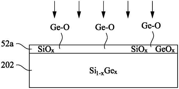
forming a silicon germanium layer on a substrate;
oxidizing a surface layer of the silicon germanium layer to form an interfacial layer comprising silicon oxide and germanium oxide;
nitridating the interfacial layer; and
forming a metal gate structure over the nitridated interfacial layer.