| CPC H01L 29/78696 (2013.01) [H01L 27/127 (2013.01); H01L 27/1222 (2013.01); H01L 29/1033 (2013.01); H01L 29/1037 (2013.01); H01L 29/42384 (2013.01); H01L 29/4908 (2013.01); H01L 29/66545 (2013.01); H01L 29/66742 (2013.01); H01L 29/66772 (2013.01); H01L 29/78 (2013.01); H01L 29/7842 (2013.01); H01L 29/78654 (2013.01)] | 6 Claims |
|
1. A process for fabricating a field-effect transistor including an active zone comprising a source, a channel, a drain, and a control gate, which is positioned level with said channel, allowing a flow of charge carriers in the channel to be controlled, comprising the following steps:
producing the field-effect transistor including the source, the channel, the drain and a sacrificial gate above the channel, the channel being compressively or tensilely strained;
depositing a dielectric layer to encapsulate the field-effect transistor with a dielectric;
selectively etching the sacrificial gate so as to define a gate cavity through the encapsulating dielectric layer;
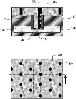
depositing a block copolymer layer comprising a first species and a second species in the gate cavity having a source-side first internal wall and a drain-side second internal wall;
removing the first or second species so as to define masking patterns positioned facing at least one of the walls and opening onto the bottom of the gate cavity;
producing one or more perforations in the channel facing said wall or said walls;
depositing at least one gate material in the gate cavity facing the perforated channel,
wherein the process comprises the depositing of a neutralizing layer prior to the deposition of the block copolymer layer, so as to allow the one or more perforations in the channel to be given a preferred orientation.
|