|
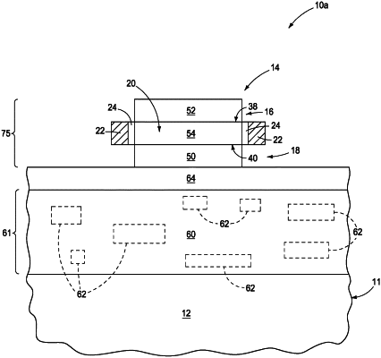
1. A method of forming integrated circuitry, comprising: forming operative circuit components above a substrate; forming an insulator material directly above the operative circuit components; forming a bottom material, a top material, and a middle material vertically between the bottom and top materials directly above the insulator material; the bottom, top, and middle materials respectively comprising a bottom source/drain region, a top source/drain region, and a channel region vertically between the bottom and top source/drain regions in a finished construction of a transistor that will be directly above the insulator material; at least the bottom and the top materials comprising conductivity-increasing dopant therein in the finished construction of the transistor; laser annealing at least one of the bottom, top, and middle materials to melt and then crystallize the at least one of the bottom, top, and middle materials to be crystalline; the laser annealing activating the conductivity-increasing dopant that is in the at least one of the bottom, top, and middle materials; the insulator material that is vertically between the operative circuit components and the bottom material shielding the operative circuit components there-below from heat generated during the laser annealing that would otherwise render the operative circuit components to become circuit inoperative; and forming a gate insulator and a gate laterally-adjacent the middle material.
|
