| CPC H01L 29/7839 (2013.01) [H01L 21/823814 (2013.01); H01L 21/823821 (2013.01); H01L 27/0924 (2013.01); H01L 29/0847 (2013.01); H01L 29/41791 (2013.01); H01L 29/66545 (2013.01); H01L 29/66795 (2013.01); H01L 29/7851 (2013.01)] | 20 Claims |
|
1. A device comprising:
a first fin extending from a substrate;
a first gate stack over and along sidewalls of the first fin;
a first gate spacer disposed along a sidewall of the first gate stack; and
a first source/drain region in the first fin and adjacent the first gate spacer, the first source/drain region comprising:
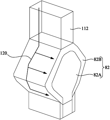
a first epitaxial layer on the first fin, the first epitaxial layer having a first dopant concentration of boron; and
a second epitaxial layer on the first epitaxial layer, the second epitaxial layer having a second dopant concentration of boron, the second dopant concentration being greater than the first dopant concentration, the second epitaxial layer being an outermost layer of the first source/drain region.
|