| CPC H01L 29/7816 (2013.01) [H01L 29/0653 (2013.01); H01L 29/0692 (2013.01); H01L 29/402 (2013.01); H01L 29/41758 (2013.01); H01L 29/66681 (2013.01)] | 20 Claims |
|
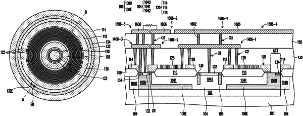
1. A semiconductor device, comprising:
a drain region in a substrate;
a source region in the substrate, completely surrounding the drain region;
a gate structure, disposed on the substrate, disposed between the source region and the drain region and surrounding the drain region; and
a metallic line, located above the source and drain regions and the gate structure and electrically connected to the drain region or the source region,
wherein the source region includes a doped region having a break region located between two opposite ends of the doped region, and
wherein the metallic line extends from the drain region, across the gate structure and across the break region and beyond the source region.
|