| CPC H01L 29/7786 (2013.01) [H01L 29/2003 (2013.01); H01L 29/66462 (2013.01)] | 13 Claims |
|
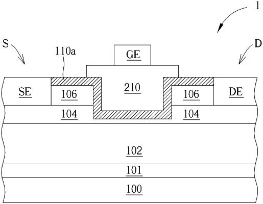
1. A method for forming a high electron mobility transistor, comprising:
providing a substrate;
forming a channel layer on the substrate;
forming an electron supply layer on the channel layer;
forming a dielectric passivation layer on the electron supply layer;
forming a gate recess into the dielectric passivation layer and the electron supply layer;
conformally depositing a surface modification layer on an interior surface of the gate recess;
subjecting the surface modification layer to an oxidation treatment or a nitridation treatment, wherein the surface modification layer is first subjected to the oxidation treatment and is then subjected to the nitridation treatment; and
forming a P-type GaN layer in the gate recess and on the surface modification layer.
|