| CPC H01L 29/6681 (2013.01) [H01L 21/823431 (2013.01); H01L 29/0669 (2013.01); H01L 29/66545 (2013.01); H01L 29/7851 (2013.01)] | 20 Claims |
|
1. A method of forming a semiconductor device, comprising:
forming a fin structure having a stack of alternating first semiconductor layers and second semiconductor layers over a substrate, the first semiconductor layers and the second semiconductor layers having different compositions;
forming a dummy gate structure across the fin structure;
forming gate spacers on opposite sidewalls of the dummy gate structure, respectively;
removing the dummy gate structure to form a gate trench between the gate spacers;
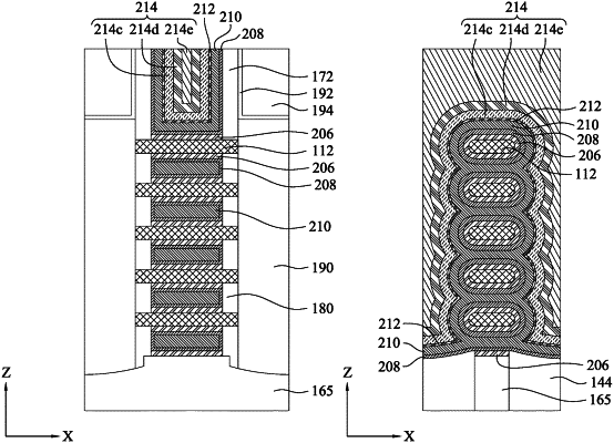
etching the first semiconductor layers in the gate trench, such that the second semiconductor layers are suspended in the gate trench to serve as nanosheets;
forming a work function metal layer surrounding each of the nanosheets, wherein the work function metal layer on adjacent nanosheets merges as a single continuous layer, and wherein from a cross-sectional view, each of the nanosheets has arc-shaped sides, and the single continuous layer has repeating arc patterns corresponding to the arc-shaped sides of the nanosheets in a one-to-one manner;
forming a glue layer on the work function metal layer, wherein the glue layer has a thickness less than a thickness of the work function metal layer; and
depositing a fill metal layer over the work function metal layer without using a fluorine-containing precursor, wherein depositing the fill metal layer comprises:
conformally forming a first fluorine-free metal sublayer over the glue layer, wherein the first fluorine-free metal sublayer comprises TaN,
conformally forming a second fluorine-free metal sublayer over the first fluorine-free metal sublayer, wherein the second fluorine-free metal sublayer comprises TiN or tungsten; and
forming a third fluorine-free metal sublayer over the second fluorine-free metal sublayer.
|