| CPC H01L 29/66636 (2013.01) [H01L 21/02507 (2013.01); H01L 21/02532 (2013.01); H01L 21/3065 (2013.01); H01L 21/764 (2013.01); H01L 21/823814 (2013.01); H01L 21/823821 (2013.01); H01L 21/823878 (2013.01); H01L 27/0924 (2013.01); H01L 29/0653 (2013.01); H01L 29/0847 (2013.01); H01L 29/165 (2013.01); H01L 29/66545 (2013.01); H01L 29/7848 (2013.01); H10B 10/12 (2023.02); H10B 10/18 (2023.02)] | 20 Claims |
|
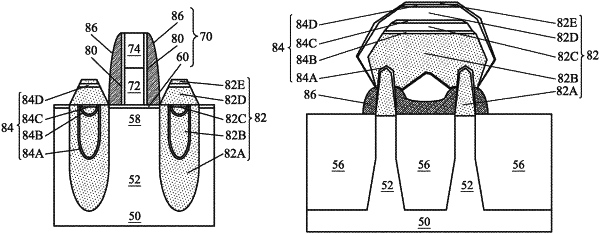
1. A semiconductor device, comprising:
a first semiconductor fin and a second semiconductor fin, the first semiconductor fin and the second semiconductor fin extending from a substrate;
a gate electrode over the first semiconductor fin and the second semiconductor fin; and
a source/drain region adjacent to the gate electrode and over the first semiconductor fin and the second semiconductor fin, wherein a top surface of the source/drain region is higher than a top surface of the first semiconductor fin and the second semiconductor fin under the gate electrode, wherein the source/drain region comprises a plurality of buffer layers and a plurality of body layers, wherein the source/drain region comprises alternating layers of a buffer layer of the plurality of buffer layers and a body layer of the plurality of body layers, wherein a lower sidewall of a first body layer of the plurality of body layers is covered by a second body layer of the plurality of body layers, wherein at least one body layer of the plurality of body layers is free of facets.
|