| CPC H01L 29/66462 (2013.01) [H01L 29/2003 (2013.01); H01L 29/4236 (2013.01); H01L 29/42364 (2013.01); H01L 29/7786 (2013.01)] | 12 Claims |
|
1. A high electron mobility transistor (HEMT) comprising:
a first III-V compound layer;
a second III-V compound layer disposed on the first III-V compound layer, wherein a composition of the first III-V compound layer is different from a composition of second III-V compound layer;
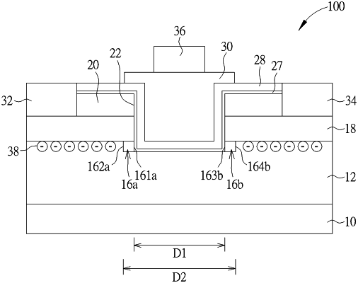
a trench disposed within the first III-V compound layer and the second III-V compound layer, wherein the trench has a first corner and a second corner both disposed within the first III-V compound layer, the first corner is formed by a first sidewall and a bottom of the trench and the second corner is formed by a second sidewall and the bottom of the trench;
a first dielectric layer contacting the first sidewall and a second dielectric layer contacting the second sidewall, wherein the first dielectric layer and the second dielectric layer are both disposed outside of the trench;
a gate disposed in the trench;
a source electrode disposed at one side of the gate;
a drain electrode disposed at another side of the gate; and
a gate electrode disposed directly on the gate.
|