US 11,688,789 B2
Semiconductor device with reduced flicker noise
Hsin-Li Cheng, Hsin Chu (TW); Liang-Tai Kuo, Zhudong Township (TW); and Yu-Chi Chang, Kaohsiung (TW)
Assigned to Taiwan Semiconductor Manufacturing Company, Ltd., Hsinchu (TW)
Filed by Taiwan Semiconductor Manufacturing Co., Ltd., Hsin-Chu (TW)
Filed on Mar. 11, 2021, as Appl. No. 17/198,626.
Application 16/732,397 is a division of application No. 16/117,166, filed on Aug. 30, 2018, granted, now 10,529,818, issued on Jan. 7, 2020.
Application 17/198,626 is a continuation of application No. 16/732,397, filed on Jan. 2, 2020, granted, now 10,971,596.
Claims priority of provisional application 62/703,636, filed on Jul. 26, 2018.
Prior Publication US 2021/0202711 A1, Jul. 1, 2021
This patent is subject to a terminal disclaimer.
Int. Cl. H01L 29/66 (2006.01); H01L 29/51 (2006.01); H01L 21/3115 (2006.01); H01L 21/324 (2006.01)
CPC H01L 29/513 (2013.01) [H01L 21/31155 (2013.01); H01L 21/324 (2013.01); H01L 29/6656 (2013.01); H01L 29/66492 (2013.01)] 20 Claims
OG exemplary drawing
 
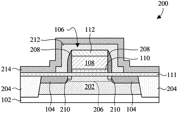
1. A semiconductor device, comprising:
source/drain regions disposed in a semiconductor substrate, wherein the source/drain regions are laterally spaced;
a gate stack disposed over the semiconductor substrate and disposed between the source/drain regions;
a cap layer disposed over the gate stack, wherein a first lower surface of the cap layer contacts a first upper surface of the gate stack;
sidewall spacers disposed along sides of the gate stack;
a first dielectric layer disposed over the cap layer, wherein the first dielectric layer extends along sides of the sidewall spacers toward the semiconductor substrate; and
a second dielectric layer disposed over the first dielectric layer and over the source/drain regions.