| CPC H01L 29/4966 (2013.01) [H01L 21/02697 (2013.01); H01L 29/42368 (2013.01); H01L 29/42376 (2013.01); H01L 29/4958 (2013.01); H01L 29/66545 (2013.01); H01L 29/78 (2013.01); H01L 29/517 (2013.01); H01L 29/7833 (2013.01)] | 20 Claims |
|
1. A semiconductor device, comprising:
a semiconductor substrate having a top surface; and
a gate structure disposed over the semiconductor substrate, wherein the gate structure includes:
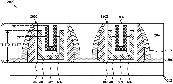
a gate dielectric layer of a substantially U-shaped configuration and extending to a first height above the top surface, wherein the substantially U-shaped configuration has a bottom portion, a first side portion extending up from a first end of the bottom portion and a second side portion extending up from a second end of the bottom portion;
a first metal layer directly on the gate dielectric layer, wherein the first metal layer interfaces a top surface of the bottom portion, a first portion of a sidewall of the first side portion, and a second portion of a sidewall of the second side portion; and
a second metal layer over the first metal layer and extending to a second height above the top surface, wherein the second height is greater than the first height, and wherein the second metal layer interfaces a top surface of the first side portion and a top surface of the second side portion of the gate dielectric layer.
|