US 11,688,784 B2
Transistor layout to reduce kink effect
Meng-Han Lin, Hsinchu (TW); Te-Hsin Chiu, Miaoli County (TW); and Wei Cheng Wu, Zhubei (TW)
Assigned to Taiwan Semiconductor Manufacturing Company, Ltd., Hsinchu (TW)
Filed by Taiwan Semiconductor Manufacturing Co., Ltd., Hsin-Chu (TW)
Filed on Mar. 31, 2021, as Appl. No. 17/218,307.
Application 17/218,307 is a continuation of application No. 16/661,108, filed on Oct. 23, 2019, granted, now 10,971,590.
Application 16/661,108 is a continuation of application No. 15/989,606, filed on May 25, 2018, granted, now 10,510,855, issued on Dec. 17, 2019.
Claims priority of provisional application 62/585,636, filed on Nov. 14, 2017.
Prior Publication US 2021/0217868 A1, Jul. 15, 2021
This patent is subject to a terminal disclaimer.
Int. Cl. H01L 29/00 (2006.01); H01L 29/423 (2006.01); H01L 29/10 (2006.01); H01L 29/78 (2006.01); H01L 29/08 (2006.01); H01L 29/66 (2006.01); H01L 21/762 (2006.01); H01L 29/06 (2006.01); H01L 21/28 (2006.01)
CPC H01L 29/42376 (2013.01) [H01L 21/28123 (2013.01); H01L 21/76224 (2013.01); H01L 29/0692 (2013.01); H01L 29/0847 (2013.01); H01L 29/1033 (2013.01); H01L 29/4238 (2013.01); H01L 29/6659 (2013.01); H01L 29/66598 (2013.01); H01L 29/7833 (2013.01); H01L 29/7834 (2013.01); H01L 29/665 (2013.01)] 20 Claims
OG exemplary drawing
 
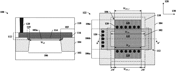
1. An integrated chip, comprising:
an isolation structure arranged within a substrate and having one or more surfaces defining one or more trenches that are recessed below an uppermost surface of the isolation structure and that are disposed along opposing sides of an active region of the substrate; and
a conductive gate arranged over the substrate between a source region and a drain region, wherein the conductive gate extends into the one or more trenches disposed along the opposing sides of the active region of the substrate, and wherein the conductive gate has an upper surface that continuously extends past opposing sides of the one or more trenches.