| CPC H01L 29/41791 (2013.01) [H01L 21/76224 (2013.01); H01L 21/823425 (2013.01); H01L 21/823431 (2013.01); H01L 27/0886 (2013.01)] | 19 Claims |
|
1. A semiconductor device comprising:
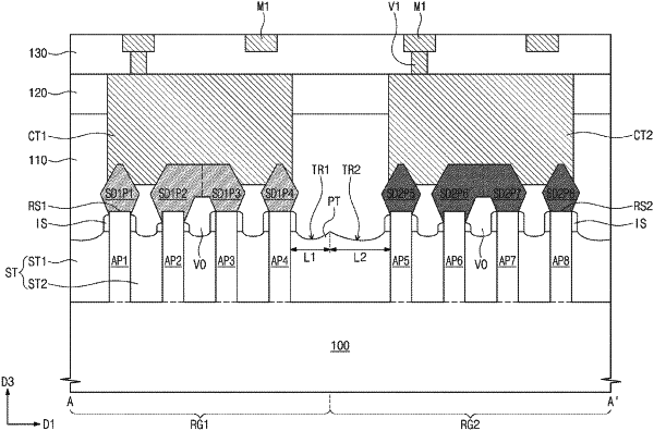
a substrate including a first region and a second region;
a first fin, a second fin, a third fin and a fourth fin on the first region of the substrate;
a fifth fin, a sixth fin, a seventh fin and an eighth fin on the second region of the substrate;
a first isolation on the first region of the substrate;
a second isolation on the first region of the substrate, and between the first fin and the second fin, the first fin between the first isolation and the second isolation;
a third isolation on the first region of the substrate, and between the second fin and the third fin;
a fourth isolation on the first region of the substrate, and between the third fin and the fourth fin;
a fifth isolation on the substrate, and between the fourth fin and the fifth fin;
a sixth isolation on the second region of the substrate, and between the fifth fin and the sixth fin;
a seventh isolation on the second region of the substrate, and between the sixth fin and the seventh fin;
an eighth isolation on the second region of the substrate, and between the seventh fin and the eighth fin;
a ninth isolation on the second region of the substrate, the eighth fin being between the eighth isolation and the ninth isolation;
a first gate on the first through eighth fins and the first through ninth isolations;
a second gate on the first through eighth fins and the first through ninth isolations;
a first epitaxial source/drain on the first fin, and between the first gate and the second gate;
a second epitaxial source/drain on the second fin, and between the first gate and the second gate;
a third epitaxial source/drain on the third fin, and between the first gate and the second gate;
a fourth epitaxial source/drain on the fourth fin, and between the first gate and the second gate;
a fifth epitaxial source/drain on the fifth fin, and between the first gate and the second gate;
a sixth epitaxial source/drain on the sixth fin, and between the first gate and the second gate;
a seventh epitaxial source/drain on the seventh fin, and between the first gate and the second gate;
an eighth epitaxial source/drain on the eighth fin, and between the first gate and the second gate;
a first spacer on a sidewall of the first fin;
a second spacer on a sidewall of the second fin;
a third spacer on a sidewall of the third fin;
a fourth spacer on a sidewall of the fourth fin;
a fifth spacer on a sidewall of the fifth fin;
a sixth spacer on a sidewall of the sixth fin;
a seventh spacer on a sidewall of the seventh fin;
an eighth spacer on a sidewall of the eighth fin;
a first contact on the first through fourth epitaxial source/drains; and
a second contact on the fifth through eighth epitaxial source/drains,
wherein the second epitaxial source/drain and the third epitaxial source/drain are merged,
wherein the sixth epitaxial source/drain and the seventh epitaxial source/drain are merged,
wherein a height of the second spacer is different from a height of the third spacer, and
wherein a minimum distance between an upper surface of the substrate and a lowermost portion of the second epitaxial source/drain is different from a minimum distance between the upper surface of the substrate and a lowermost portion of the third epitaxial source/drain.
|