| CPC H01L 29/41791 (2013.01) [H01L 23/481 (2013.01); H01L 27/0886 (2013.01); H01L 29/0615 (2013.01); H01L 29/0847 (2013.01); H01L 29/401 (2013.01); H01L 29/4175 (2013.01); H01L 29/456 (2013.01); H01L 29/66492 (2013.01); H01L 29/66795 (2013.01); H01L 29/785 (2013.01); H01L 29/7833 (2013.01); H01L 2029/7858 (2013.01)] | 13 Claims |
|
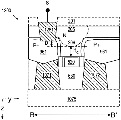
1. A transistor structure, comprising:
a fin comprising a channel region over a sub-channel region, the channel region comprising a first semiconductor material having a first impurity concentration;
a gate electrode adjacent to a sidewall of the channel region, and over a dielectric material that is adjacent to a sidewall of the sub-channel region;
a source region and a drain region on opposite sides of the gate electrode, wherein at least one of the source region and the drain region comprises:
a second semiconductor material that has a second impurity concentration greater than the first impurity concentration; and
a third semiconductor material between the second semiconductor material and the sidewall of both the channel region and the sub-channel region, the third semiconductor material having a third impurity concentration exceeding the first impurity concentration, but less than the second impurity concentration;
first contact metallization coupled to a first side of the source region or drain region, the first contact metallization in contact with the second semiconductor material; and
second contact metallization coupled to a second side of the source region or drain region, opposite the first side, the second contact metallization extending through a thickness of the third semiconductor material and in contact with the second semiconductor material.
|