| CPC H01L 29/41733 (2013.01) [H01L 29/401 (2013.01); H01L 29/66666 (2013.01); H01L 29/7827 (2013.01)] | 19 Claims |
|
1. A method of forming a semiconductor structure, comprising:
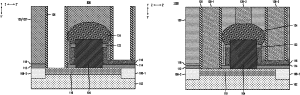
forming at least one fin disposed over a top surface of a substrate, the at least one fin providing a vertical transport channel for a vertical transport field-effect transistor;
forming a top source/drain region disposed over a top surface of the at least one fin;
forming an interlevel dielectric layer surrounding the top source/drain region and the at least one fin;
forming a first contact trench in the interlevel dielectric layer at a first end of the at least one fin for a bottom source/drain contact of the vertical transport field-effect transistor and a second contact trench in the interlevel dielectric layer at a second end of the at least one fin for a gate contact of the vertical transport field-effect transistor, the first and second contact trenches being self-aligned to the top source/drain region, the first contact trench abutting a portion of the top source/drain region at the first end of the at least one fin and the second contact trench abutting a portion of the top source/drain region at the second end of the at least one fin;
forming inner spacers on sidewalls of the first contact trench and the second contact trench; and
forming contact material in the first contact trench and the second contact trench between the inner spacers;
wherein the contact material comprises a stressor material that induces vertical strain in the at least one fin.
|