| CPC H01L 29/0847 (2013.01) [H01L 21/0262 (2013.01); H01L 21/02636 (2013.01); H01L 21/3065 (2013.01); H01L 29/66628 (2013.01); H01L 29/66636 (2013.01); H01L 29/7848 (2013.01); H01L 21/02532 (2013.01); H01L 29/045 (2013.01); H01L 29/165 (2013.01); H01L 29/665 (2013.01); H01L 29/66545 (2013.01)] | 20 Claims |
|
1. A semiconductor device structure, comprising:
a gate stack over a semiconductor substrate;
a source/drain structure adjacent to the gate stack; and
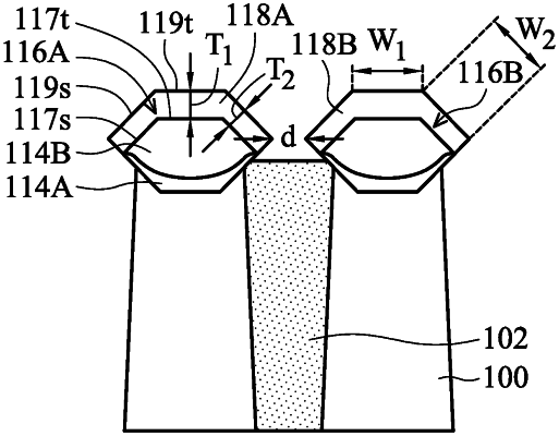
a cap element over the source/drain structure, wherein:
the cap element has a first top plane,
the source/drain structure has a second top plane,
the first top plane of the cap element is substantially parallel to the second top plane of the source/drain structure,
the cap element has a first thickness measured between the first top plane and the second top plane, the cap element has a second thickness measured between the side surface of the cap element and a side surface of the source/drain structure, and the first thickness and the second thickness are different from each other,
the first top plane of the cap element is wider than the second top plane of the source/drain structure, and
a surface orientation of the first top plane of the cap element and a surface orientation of a side surface of the cap element are different from each other, and the surface orientation of the first top plane of the cap element is {311}.
|