| CPC H01L 29/0673 (2013.01) [H01L 29/0847 (2013.01); H01L 29/66439 (2013.01); H01L 29/66545 (2013.01); H01L 29/66636 (2013.01); H01L 29/775 (2013.01); H01L 29/78696 (2013.01); H01L 29/42392 (2013.01)] | 20 Claims |
|
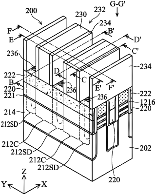
1. A device, comprising:
a semiconductor substrate having a substrate surface;
a stack of channel layers on the semiconductor substrate;
a gate structure engaging with the stack of channel layers and extending along a first direction;
a gate spacer on sidewalls of the gate structure;
a source/drain feature on first sidewall surfaces of the stack of channel layers and on the substrate, the first sidewall surfaces extending in parallel to the first direction; and
a first dielectric feature directly contacting the source/drain feature and second sidewall surfaces of the stack of channel layers, the second sidewall surfaces extending perpendicular to the first direction,
wherein the gate spacer is in direct contact with a topmost channel layer in the stack of channel layers,
wherein the source/drain feature has a top portion having a first width along the first direction and a bottom portion having a second width along the first direction, and wherein the first width is greater than the second width.
|