| CPC H01L 29/0673 (2013.01) [H01L 29/66553 (2013.01); H01L 29/7848 (2013.01)] | 20 Claims |
|
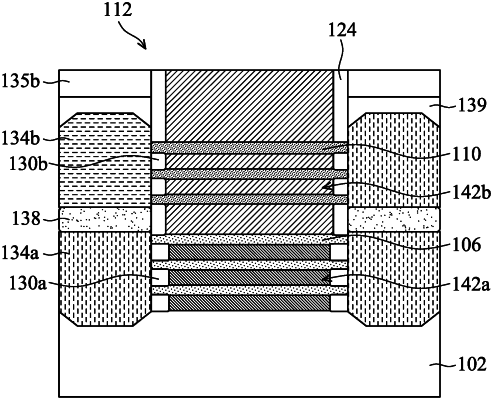
1. A semiconductor device structure, comprising:
first nanostructures formed over a substrate;
a first gate structure wrapped around the first nanostructures;
first source/drain epitaxial structures formed over opposite sides of the first nanostructures;
second nanostructures formed over the first nanostructure;
a second gate structure wrapped around the second nanostructures;
second source/drain epitaxial structures formed over opposite sides of the second nanostructures;
a power rail formed below a bottom surface of the first source/drain epitaxial structures and electrically connected to the first source/drain epitaxial structures,
a first inner spacer formed beside the first gate structure; and
a second inner spacer formed beside the second gate structure,
wherein the first inner spacer is wider than the second inner spacer;
wherein the first gate structure and the second gate structure have different conductivity types, and a Ge concentration of the first nanostructures and a Ge concentration of the second nanostructures are different.
|