US 11,688,766 B2
Seal material for air gaps in semiconductor devices
Shuen-Shin Liang, Hsinchu County (TW); Chen-Han Wang, Hsinchu County (TW); Keng-Chu Lin, Ping-Tung (TW); Tetsuji Ueno, Hsinchu (JP); and Ting-Ting Chen, New Taipei (TW)
Assigned to Taiwan Semiconductor Manufacturing Co., Ltd., Hsinchu (TW)
Filed by Taiwan Semiconductor Manufacturing Co., Ltd., Hsinchu (TW)
Filed on Apr. 4, 2022, as Appl. No. 17/712,234.
Application 17/712,234 is a continuation of application No. 16/937,344, filed on Jul. 23, 2020, granted, now 11,296,187.
Claims priority of provisional application 62/951,852, filed on Dec. 20, 2019.
Prior Publication US 2022/0223686 A1, Jul. 14, 2022
This patent is subject to a terminal disclaimer.
Int. Cl. H01L 29/06 (2006.01); H01L 21/02 (2006.01); H01L 29/78 (2006.01); H01L 29/417 (2006.01); H01L 29/66 (2006.01); H01L 27/088 (2006.01)
CPC H01L 29/0653 (2013.01) [H01L 21/02447 (2013.01); H01L 21/02529 (2013.01); H01L 27/0886 (2013.01); H01L 29/41791 (2013.01); H01L 29/66795 (2013.01); H01L 29/7851 (2013.01)] 20 Claims
OG exemplary drawing
 
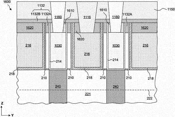
1. A semiconductor device, comprising:
a gate electrode on a fin region;
a source/drain (S/D) structure on the fin region;
an etch stop layer on a sidewall of the S/D structure;
a seal layer between the gate electrode and the etch stop layer, wherein the seal layer comprises a silicon carbide material doped with oxygen; and
an air gap in physical contact with the etch stop layer and surrounded by the seal layer, the fin region, the gate electrode, and the S/D structure.