| CPC H01L 28/91 (2013.01) [H01L 21/0274 (2013.01); H01L 21/30604 (2013.01); H01L 21/31053 (2013.01); H01L 21/31111 (2013.01); H01L 21/3212 (2013.01); H01L 21/32055 (2013.01); H01L 21/32133 (2013.01); H01L 21/764 (2013.01); H01L 23/562 (2013.01); H01L 27/016 (2013.01); H01L 28/87 (2013.01); H01L 28/92 (2013.01); H01L 29/66181 (2013.01); H01L 29/945 (2013.01); H10B 12/0387 (2023.02); H10B 12/37 (2023.02); H01L 27/0805 (2013.01); H01L 2224/13101 (2013.01); H01L 2224/2919 (2013.01); H01L 2224/32145 (2013.01); H01L 2224/32225 (2013.01); H01L 2224/48091 (2013.01); H01L 2224/48227 (2013.01); H01L 2224/73204 (2013.01); H01L 2224/73265 (2013.01); H01L 2924/00014 (2013.01); H01L 2924/1304 (2013.01); H01L 2924/1305 (2013.01); H01L 2924/13091 (2013.01); H01L 2924/14 (2013.01); H01L 2924/15311 (2013.01); H01L 2924/181 (2013.01); H01L 2924/19011 (2013.01); H01L 2924/19103 (2013.01); H01L 2924/19105 (2013.01); H01L 2924/3511 (2013.01)] | 20 Claims |
|
1. A semiconductor die, comprising:
a substrate;
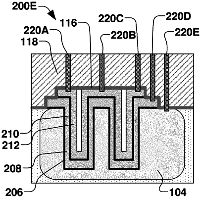
a trench array having a plurality of capacitor trench segments disposed in the substrate, wherein the plurality of capacitor trench segments are rotationally symmetric about a center (CNTR) of the trench array;
a first dielectric layer contacting a bottom region and sidewalls of the plurality of capacitor trench segments;
a first conducting layer disposed in the plurality of capacitor trench segments, wherein the first conducting layer is insulated from the substrate by the first dielectric layer, and further wherein the first conducting layer has a first thickness that is substantially uniform along the bottom region and the sidewalls of the plurality of capacitor trench segments;
a second conducting layer disposed over the first conducting layer and insulated from the first conducting layer by a second dielectric layer; and
air gaps disposed in the second conducting layer, wherein dimensions of the air gaps maintain the second conducting layer with a second thickness that is substantially uniform along the bottom region and the sidewalls of the plurality of capacitor trench segments and the second thickness is substantially equal to the first thickness.
|