| CPC H01L 28/82 (2013.01) [G06F 30/10 (2020.01); H01G 4/306 (2013.01)] | 11 Claims |
|
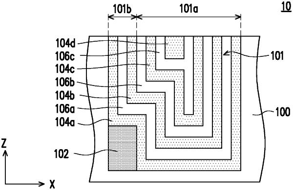
1. A multilayer capacitive element, comprising:
a substrate having a groove;
a first aspect ratio modulation structure located in the groove to define the groove as a first region and a first modulation region, wherein an aspect ratio of the first modulation region is different from an aspect ratio of the first region; and
a plurality of conductive layers and a plurality of dielectric layers alternately stacked in the groove,
wherein at least one of the plurality of conductive layers is only disposed in the first region and not disposed in the first modulation region, in a top view,
wherein at least one conductive layer in the plurality of conductive layers is extended from the first region to the first modulation region, in a top view,
wherein a topmost conductive layer in the at least one conductive layer extended from the first region to the first modulation region completely fills a space of the groove of the first modulation region, in top view, and
wherein the plurality of conductive layers and the plurality of dielectric layers are not disposed on a top surface of the first aspect ratio modulation structure.
|