| CPC H01L 27/14643 (2013.01) [H01L 27/1462 (2013.01); H01L 27/1464 (2013.01); H01L 27/14627 (2013.01); H01L 27/14629 (2013.01); H01L 27/14634 (2013.01); H01L 27/14636 (2013.01); H01L 27/14685 (2013.01)] | 20 Claims |
|
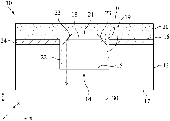
1. A photonic device, comprising:
a substrate having a first surface and a cavity extending into the substrate from the first surface to a second surface;
a semiconductor layer on the second surface in the cavity of the substrate;
a cover layer on the semiconductor layer; and
sidewall spacers between side surfaces of the cavity and side surfaces of the semiconductor layer,
wherein the semiconductor layer is configured to receive incident radiation through the substrate and to totally internally reflect the radiation at an interface between the semiconductor layer and the cover layer.
|