| CPC H01L 27/14612 (2013.01) [H01L 27/1463 (2013.01); H01L 27/14603 (2013.01); H01L 27/14623 (2013.01); H01L 27/14643 (2013.01); H01L 27/14656 (2013.01)] | 15 Claims |
|
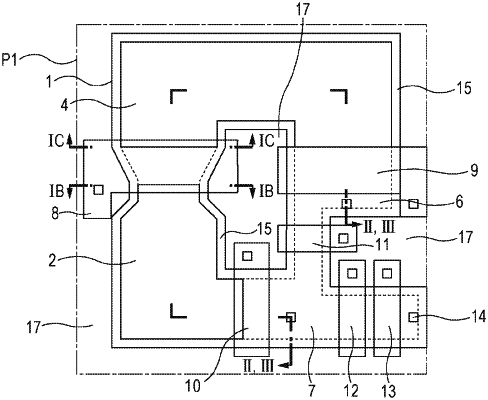
1. A photoelectric conversion apparatus in which a plurality of pixels are laid out in a matrix form, each of the pixels having a photoelectric conversion portion, a first transfer transistor configured to transfer electric carriers from the photoelectric conversion portion, an electric-carrier accumulation portion to which the electric carriers are transferred by the first transfer transistor, a second transfer transistor configured to transfer electric carriers accumulated in the electric-carrier accumulation portion, and a floating diffusion to which the electric carriers are transferred by the second transfer transistor, the photoelectric conversion apparatus comprising:
an active region having the photoelectric conversion portion, the electric-carrier accumulation portion, and the floating diffusion; and
an element isolation region having an insulator defining the active region;
wherein the first transfer transistor is provided at a position closest to the photoelectric conversion portion among a plurarity of transistors including the first transfer transistor and the second transfer transistor arranged in an electric-carrier transfer path from the photoelectric conversion portion to the floating diffusion, and
wherein, in a predetermined direction in plan view, a first total length from a first boundary where the element isolation region contacts the active region to a second boundary where the element isolation region contacts the active region in the electric carrier accumulation portion under a gate of the first transfer transistor is larger than a second total length from a third boundary where the element isolation region contacts the active region to a fourth boundary where the element isolation region contacts the active region in the photoelectric conversion portion under the gate of the first transfer transistor, and
wherein, in the predetermined direction in plan view, the active region in the photoelectric conversion portion has a third total length from a fifth boundary where the element isolation region contacts the active region to a sixth boundary where the element isolation region contacts the active region, the third total length being larger than the second total length.
|