| CPC H01L 27/1225 (2013.01) [H01L 21/02565 (2013.01); H01L 27/127 (2013.01); H01L 27/1251 (2013.01); H01L 27/1255 (2013.01); H01L 29/66969 (2013.01); H01L 29/7869 (2013.01); H01L 29/78696 (2013.01); H10K 59/1213 (2023.02)] | 20 Claims |
|
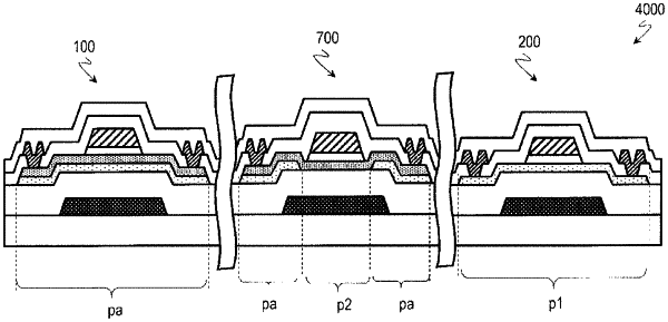
1. An active matrix substrate having a display region including a plurality of pixel areas and a non-display region arranged around the display region, the active matrix substrate comprising:
a substrate; and
a plurality of oxide semiconductor TFTs supported on the substrate and provided in the display region or the non-display region, each of the plurality of oxide semiconductor TFTs includes an oxide semiconductor layer and a gate electrode arranged on a part of the oxide semiconductor layer with a gate insulating layer interposed between the oxide semiconductor layer and the gate electrode,
wherein the oxide semiconductor layer has a first region covered with the gate electrode with the gate insulating layer interposed between the oxide semiconductor layer and the gate electrode,
a first TFT and a second TFT are included in the plurality of oxide semiconductor TFTs,
in the first TFT, in the first region, the oxide semiconductor layer has a layered structure including a lower oxide semiconductor film and an upper oxide semiconductor film arranged on the lower oxide semiconductor film throughout and a mobility of the upper oxide semiconductor film is higher than a mobility of the lower oxide semiconductor film,
in the second TFT, in at least a part of the first region of the oxide semiconductor layer, of the lower oxide semiconductor film and the upper oxide semiconductor film, one oxide semiconductor film is provided and another oxide semiconductor film is not provided, and
in the at least a part of the first region in the second TFT, the lower oxide semiconductor film is provided and the upper oxide semiconductor film is not provided.
|