| CPC H01L 27/0886 (2013.01) [H01L 21/76224 (2013.01); H01L 21/823412 (2013.01); H01L 21/823431 (2013.01); H01L 29/0665 (2013.01); H01L 29/6681 (2013.01); H01L 29/7851 (2013.01); H01L 29/7855 (2013.01)] | 20 Claims |
|
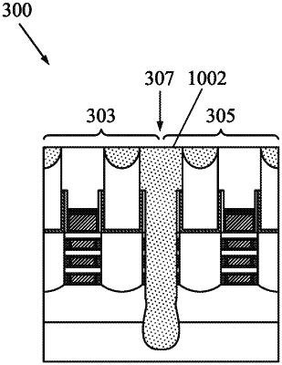
1. A method of fabricating a semiconductor device, comprising:
etching a metal layer from a dummy gate structure disposed at an active edge, wherein the etching the metal layer removes the metal layer from between adjacent channel layers, and wherein a gate dielectric layer of the dummy gate structure remains disposed between the adjacent channel layers after removal of the metal layer; and
after etching the metal layer from the dummy gate structure, forming a cut region along the active edge, wherein a portion of the gate dielectric layer remains disposed at a channel layer-inner spacer interface after formation of the cut region.
|