| CPC H01L 27/0207 (2013.01) [H01L 21/32133 (2013.01); H01L 21/32139 (2013.01); H01L 21/823431 (2013.01); H01L 21/823475 (2013.01); H01L 27/0886 (2013.01); H01L 29/41791 (2013.01); H01L 29/42376 (2013.01); H01L 21/823437 (2013.01); H01L 27/1104 (2013.01); H01L 27/1116 (2013.01)] | 20 Claims |
|
1. A system for manufacturing a semiconductor device, the system comprising:
at least one processor; and
at least one memory including computer program code for one or more programs;
wherein the at least one memory, the computer program code and the at least one processor are configured to cause the system to execute:
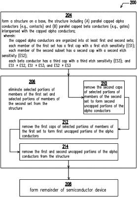
generating a layout diagram, the layout diagram being stored on a non-transitory computer-readable medium, the generating the layout diagram including:
generating fin shapes, long axes of the fin shapes extending substantially parallel to a first direction;
generating first and second conductor shapes correspondingly over the fin shapes, long axes of the first and second conductor shapes extending substantially parallel to a second direction, the second direction being substantially perpendicular to the first direction;
arranging a first sequence of alternating ones of the first and second conductor shapes relative to the first direction;
inserting a corresponding one of the second conductor shapes between each neighboring pair of corresponding ones of the first conductor shapes;
generating first, second, and third cap shapes correspondingly over the first and second conductor shapes, long axes of the first, second, and third cap shapes extending substantially parallel to the second direction;
generating first cut patterns over selected portions of corresponding ones of the first cap shapes and over corresponding portions of corresponding neighboring ones of the third cap shapes;
designating the first cut patterns as selective for a first etch sensitivity corresponding to the first cap shapes;
generating second cut patterns over selected portions of corresponding ones of the second cap shapes and over corresponding portions of corresponding neighboring ones of the third cap shapes; and
designating the second cut patterns as selective for a second etch sensitivity corresponding to the second cap shapes.
|