| CPC H01L 25/167 (2013.01) [H01L 24/13 (2013.01); H01L 27/124 (2013.01); H01L 2224/13016 (2013.01); H01L 2224/1319 (2013.01); H01L 2224/13083 (2013.01); H01L 2224/13124 (2013.01); H01L 2224/13147 (2013.01)] | 18 Claims |
|
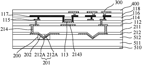
1. A display backplate, comprising:
an array substrate and a plurality of pairs of connection structures on a surface of the array substrate; wherein
the array substrate comprises a plurality of thin-film transistors and a common electrode signal line, wherein at least one of the plurality of thin-film transistors is connected to one of a pair of connection structures, and the common electrode signal line is connected to the other of the pair of the connection structures; and
an area of a first section of the connection structure is negatively correlated with a distance between the first section and the surface of the array substrate, and the first section is parallel to the surface of the array substrate,
wherein the display backplate further comprises a base disposed on the surface of the array substrate, wherein the base comprises recesses in one-to-one correspondence with the connection structures; an area of a second section of the recess is negatively correlated with a distance between the second section and the surface of the array substrate; the second section is parallel to the surface of the array substrate; and the connection structure is inside the corresponding recess.
|