| CPC H01L 25/0657 (2013.01) [H01L 21/56 (2013.01); H01L 23/3121 (2013.01); H01L 23/3135 (2013.01); H01L 23/5384 (2013.01); H01L 24/05 (2013.01); H01L 25/50 (2013.01)] | 20 Claims |
|
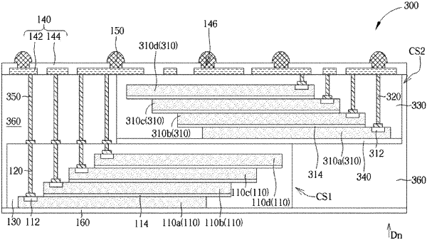
1. A chip package structure, comprising:
a chip stack comprising:
multiple chips stacked together, each of the multiple chips comprising a bonding pad not covered by the multiple chips;
a molding layer encapsulating the multiple chips, wherein a first subset of the multiple chips is separated from a second subset of the multiple chips by the molding layer;
a vertical conductive element extending from a surface of the molding layer reach and coupled to the bonding pad; and
a redistribution layer above the molding layer and having:
a conductive layer coupled to the vertical conductive element; and
an insulating layer over and partially exposing the conductive layer.
|