| CPC H01L 24/13 (2013.01) [H01L 23/5226 (2013.01); H01L 24/11 (2013.01); H01L 2224/1147 (2013.01); H01L 2224/13015 (2013.01); H01L 2224/13018 (2013.01); H01L 2224/13082 (2013.01)] | 20 Claims |
|
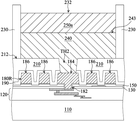
1. A chip structure, comprising:
a substrate;
a first conductive line over the substrate;
an insulating layer over the substrate and the first conductive line;
a conductive pillar over the insulating layer, wherein the conductive pillar is formed in one piece, the conductive pillar has a lower surface and a bottom protruding portion protruding from the lower surface, the bottom protruding portion passes through the insulating layer over the first conductive line, the bottom protruding portion is in direct contact with the first conductive line, and a first linewidth of a first portion of the first conductive line under the conductive pillar is less than a width of the conductive pillar; and
a solder bump on the conductive pillar, wherein the solder bump is in direct contact with the conductive pillar.
|