US 11,688,703 B2
Methods of fabricating semiconductor devices having conductive pad structures with multi-barrier films
Po-Hsun Huang, Tainan (TW); Po-Han Wang, Kaohsiung (TW); Ing-Ju Lee, Tainan (TW); Chao-Lung Chen, Tainan (TW); and Cheng-Ming Wu, Tainan (TW)
Assigned to Taiwan Semiconductor Manufacturing Company, Ltd., Hsinchu (TW)
Filed by Taiwan Semiconductor Manufacturing Company, Ltd., Hsinchu (TW)
Filed on Apr. 13, 2022, as Appl. No. 17/719,895.
Application 17/719,895 is a continuation of application No. 16/503,773, filed on Jul. 5, 2019, granted, now 11,309,265.
Claims priority of provisional application 62/711,903, filed on Jul. 30, 2018.
Prior Publication US 2022/0238467 A1, Jul. 28, 2022
This patent is subject to a terminal disclaimer.
Int. Cl. H01L 23/00 (2006.01); H01L 23/532 (2006.01); H01L 21/768 (2006.01); H01L 23/528 (2006.01)
CPC H01L 24/03 (2013.01) [H01L 21/76855 (2013.01); H01L 21/76865 (2013.01); H01L 23/5283 (2013.01); H01L 23/53223 (2013.01); H01L 23/53238 (2013.01); H01L 24/08 (2013.01)] 20 Claims
OG exemplary drawing
 
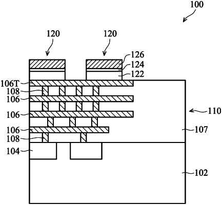
1. A method of fabricating a semiconductor device, comprising:
forming an interconnect structure over a substrate;
forming a passivation layer over the interconnect structure;
forming an opening in the passivation layer to expose a portion of the interconnect structure;
sequentially forming a lower barrier film, an upper barrier film, and an aluminum-containing layer in the opening,
wherein the lower barrier film and the upper barrier film are made of metal nitride, and the upper barrier film has a nitrogen atomic percentage that is higher than a nitrogen atomic percentage of the lower barrier film and has an amorphous structure.