| CPC H01L 23/60 (2013.01) [H01L 23/4824 (2013.01); H01L 21/02697 (2013.01); H01L 23/522 (2013.01); H01L 27/0248 (2013.01)] | 20 Claims |
|
1. A semiconductor device comprising:
a substrate having an active region that includes opposite first and second edges;
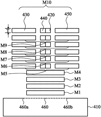
a first metallization layer disposed above the substrate, and including a first sublayer and a second sublayer, the first sublayer comprises:
a pair of first metal lines that extend from an outer periphery of the active region toward the second edge of the active region,
a first metal plate that interconnects the first metal lines and that is disposed at the outer periphery of the active region,
a pair of second metal lines, and
a second metal plate that horizontally interconnects the pair of second metal lines; and
a plurality of second metallization layers each disposed between the substrate and the first metallization layer including:
a plurality of distinct metal lines that are parallel to each other and arranged along a length of the active region underneath all of the first pair of metal lines and the second pair of metal lines, wherein the plurality of distinct metal lines have a first end at a position underneath an intermediate portion of the first metal plate, and a length that extends to a second end at a position underneath an intermediate portion of the second metal plate, wherein the plurality of distinct metal lines are of equal length to each other, and each distinct metal line of the plurality of distinct metal lines serves as a horizontal interconnect.
|