| CPC H01L 23/5389 (2013.01) [H01L 21/4853 (2013.01); H01L 21/4857 (2013.01); H01L 21/565 (2013.01); H01L 21/568 (2013.01); H01L 21/6835 (2013.01); H01L 23/3128 (2013.01); H01L 23/5383 (2013.01); H01L 23/5386 (2013.01); H01L 24/19 (2013.01); H01L 24/20 (2013.01); H01L 2221/68372 (2013.01); H01L 2224/214 (2013.01); H01L 2924/1431 (2013.01); H01L 2924/1434 (2013.01); H01L 2924/19106 (2013.01)] | 18 Claims |
|
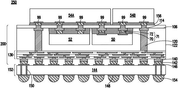
1. A package comprising:
an interposer structure free of any transistors, the interposer structure comprises:
an interconnect device;
a dielectric film surrounding the interconnect device;
first metallization pattern bonded to the interconnect device;
a second interconnect structure on an opposing side of the dielectric film as the first metallization pattern; and
a through via extending through the dielectric film, wherein the through via electrically connects the second interconnect structure to the first metallization pattern;
a first device die bonded to an opposing side of the first metallization pattern as the interconnect device;
a second device die bonded to a same side of the first metallization pattern as the first device die, wherein the interconnect device electrically connects the first device die to the second device die, wherein the interconnect device overlaps both the first device die and the second device die, and wherein the first metallization pattern comprises:
a first conductor extending continuously from a first connector of the first device die to a second connector of the interconnect device; and
a second conductor extending continuously from a third connector of the second device die to a fourth connector of the interconnect device; and
a core substrate bonded to an opposing side of the second interconnect structure as the dielectric film.
|