| CPC H01L 23/535 (2013.01) [H01L 21/76895 (2013.01); H01L 27/0207 (2013.01); H01L 27/0886 (2013.01); H01L 27/11807 (2013.01); H01L 29/785 (2013.01); H01L 2027/11875 (2013.01); H01L 2027/11881 (2013.01)] | 20 Claims |
|
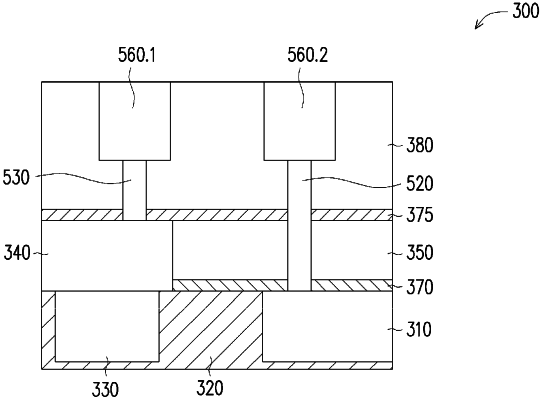
1. A method for forming a semiconductor structure, comprising:
forming a plurality of source/drain (S/D) contact structures;
depositing a first conductive material to form first and second via rail structures, wherein at least one of the first and second via rail structures is in physical contact with two or more S/D contact structures of the plurality of S/D contact structures, wherein the at least one of the first and second via rail structures extends above opposing vertical sidewalls of each of the two or more S/D contact structures of the plurality of S/D contact structures;
depositing a second conductive material to form a deep via in physical contact with the second via rail structure;
forming a first interconnect line above the first and second via rail structures and in physical contact with the first via rail structure, wherein the first interconnect line is formed in a lowest wiring level; and
forming a second interconnect line over and physically connected to the deep via, wherein the second interconnect line is in a second lowest wiring level.
|