| CPC H01L 23/53223 (2013.01) [H01L 21/0254 (2013.01); H01L 21/02458 (2013.01); H01L 21/02579 (2013.01); H01L 21/28575 (2013.01); H01L 33/04 (2013.01); H01L 33/06 (2013.01); H01L 33/145 (2013.01); H01L 33/32 (2013.01); H01L 29/205 (2013.01); H01L 31/03042 (2013.01); H01L 31/03046 (2013.01); H01L 33/305 (2013.01); H01L 33/325 (2013.01)] | 12 Claims |
|
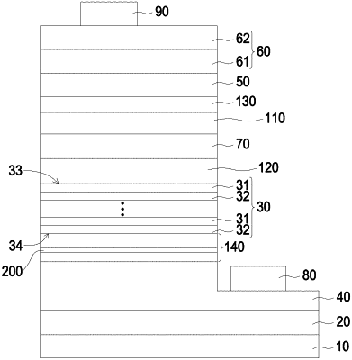
1. A semiconductor device, comprising:
a first semiconductor structure;
a second semiconductor structure on the first semiconductor structure;
an active region between the first semiconductor structure and the second semiconductor structure, wherein the active region comprises multiple alternating well layers and barrier layers, wherein each of the barrier layers has a band gap, the active region further comprises an upper surface facing the second semiconductor structure and a bottom surface opposite the upper surface;
an electron blocking region between the second semiconductor structure and the active region, wherein the electron blocking region comprises a band gap, and the band gap of the electron blocking region is greater than the band gap of one of the barrier layers;
a first aluminum-containing layer between the electron blocking region and the active region, wherein the first aluminum-containing layer has a band gap greater than the band gap of the electron blocking region;
a confinement layer between the first aluminum-containing layer and the active region, wherein the confinement layer comprises a thickness smaller than the thickness of one of the barrier layers; and
a p-type dopant above the bottom surface of the active region and comprising a concentration profile comprising a peak shape having a peak concentration value, wherein the peak concentration value lies in the electron blocking region.
|