| CPC H01L 23/5226 (2013.01) [G11C 5/06 (2013.01); G11C 11/409 (2013.01); H01L 21/486 (2013.01); H01L 21/76802 (2013.01); H01L 23/528 (2013.01); H01L 24/14 (2013.01)] | 20 Claims |
|
1. A DRAM chiplet structure, comprising:
a first hybrid bonding structure having a first surface and a second surface;
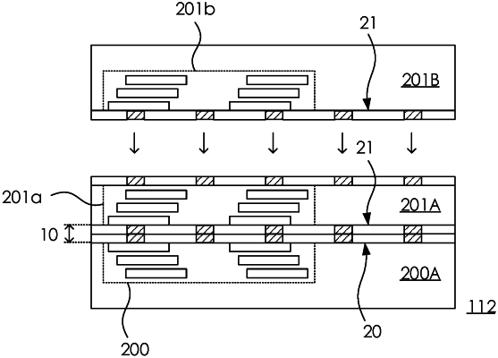
a DRAM interface structure in contact with the first surface of the first hybrid bonding structure; and
a first DRAM core structure in contact with the second surface of the first hybrid bonding structure, and the DRAM interface structure is electrically connected to the first DRAM core structure through the first hybrid bonding structure.
|