| CPC H01L 23/49822 (2013.01) [H01L 21/4857 (2013.01); H01L 23/49816 (2013.01); H01L 23/49838 (2013.01); H01L 23/552 (2013.01)] | 17 Claims |
|
1. A substrate for chip package, the substrate comprising:
a core region;
top build-up layers formed on a first side of the core region;
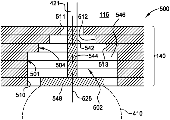
bottom build-up layers including a plurality of metal layers, the bottom build-up layers formed on a second side of the core region that is opposite the first side, routing circuitry formed in the bottom build-up layers coupled to routing circuitry formed in the top build-up layers by vias formed through the core region;
a void formed in the bottom build-up layers, the void having sectional areas that are different at least two different distances from the core region;
a first conducting structure comprising a routing trace connected to a contact pad, wherein the first conducting structure extends from the bottom build-up layers into the void; and
dielectric material filling an interstitial space defined between the routing trace and the contact pad of the first conducting structure and sidewalls of the void.
|