| CPC H01L 23/49822 (2013.01) [H01L 21/4857 (2013.01); H01L 23/49838 (2013.01); H01L 23/49816 (2013.01); H01L 23/49866 (2013.01); H01L 23/49894 (2013.01); H01L 24/16 (2013.01); H01L 24/48 (2013.01); H01L 24/73 (2013.01); H01L 2224/10175 (2013.01); H01L 2224/16227 (2013.01); H01L 2224/48227 (2013.01); H01L 2224/73257 (2013.01)] | 23 Claims |
|
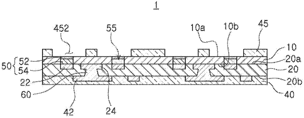
1. A printed circuit board, comprising:
a first insulating layer;
an external connection pad embedded in a first surface of the first insulating layer and having a first externally exposed surface disposed at substantially the same level as the first surface of the first insulating layer;
a second insulating layer disposed on a second surface of the first insulating layer and having a first surface in contact with the second surface of the first insulating layer; and
a first wiring pattern embedded in the second insulating layer and exposed from the first surface of the second insulating layer to be in direct contact with a second externally exposed surface of the external connection pad opposing the first externally exposed surface.
|