US 11,688,666 B2
Structures and methods for reducing process charging damages
Kuan-Jung Chen, Hsin-Chu (TW); Cheng-Hung Wang, Hsin-Chu (TW); Tsung-Lin Lee, Hsin-Chu (TW); Shiuan-Jeng Lin, Hsinchu (TW); Chun-Ming Lin, Hsin-Chu (TW); and Wen-Chih Chiang, Hsin-Chu (TW)
Assigned to Taiwan Semiconductor Manufacturing Co., Ltd., Hsin-Chu (TW)
Filed by Taiwan Semiconductor Manufacturing Co., Ltd., Hsinchu (TW)
Filed on Jun. 1, 2021, as Appl. No. 17/336,220.
Application 17/336,220 is a continuation of application No. 16/675,702, filed on Nov. 6, 2019, granted, now 11,031,320.
Claims priority of provisional application 62/773,695, filed on Nov. 30, 2018.
Prior Publication US 2021/0287963 A1, Sep. 16, 2021
This patent is subject to a terminal disclaimer.
Int. Cl. H01L 23/48 (2006.01); H01L 23/532 (2006.01); H01L 23/58 (2006.01); H01L 21/02 (2006.01); H01L 29/06 (2006.01); H01L 21/311 (2006.01); H01L 21/768 (2006.01); H01L 23/528 (2006.01); H01L 21/762 (2006.01)
CPC H01L 23/481 (2013.01) [H01L 21/02532 (2013.01); H01L 21/02595 (2013.01); H01L 21/31116 (2013.01); H01L 21/76283 (2013.01); H01L 21/76802 (2013.01); H01L 21/76877 (2013.01); H01L 23/528 (2013.01); H01L 23/53257 (2013.01); H01L 23/53271 (2013.01); H01L 23/585 (2013.01); H01L 29/0649 (2013.01)] 20 Claims
OG exemplary drawing
 
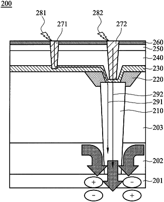
1. A semiconductor structure, comprising:
a substrate that includes:
a handle layer,
an insulation layer arranged over the handle layer, and
a buried layer arranged over the insulation layer;
a polysilicon region extending downward through the buried layer and the insulation layer, and terminating in the handle layer; and
an etch stop layer located on the substrate;
at least one contact located on the etch stop layer;
at least one dielectric layer on the etch stop layer; and
a metal layer over the at least one dielectric layer.