| CPC H01L 23/053 (2013.01) [H01L 23/04 (2013.01); H01L 23/16 (2013.01); H01L 23/3128 (2013.01); H01L 23/3675 (2013.01); H01L 23/49816 (2013.01); H01L 23/5383 (2013.01); H01L 23/5386 (2013.01); H01L 24/24 (2013.01); H01L 25/0655 (2013.01); H01L 25/165 (2013.01); H01L 25/18 (2013.01); H01L 23/367 (2013.01); H01L 23/3737 (2013.01); H01L 23/4334 (2013.01); H01L 2224/24137 (2013.01); H01L 2924/19105 (2013.01); H01L 2924/3511 (2013.01)] | 19 Claims |
|
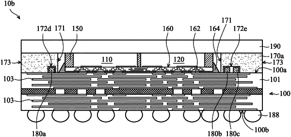
1. A semiconductor package structure, comprising:
a package substrate having a first surface and a second surface opposite to the first surface;
at least one semiconductor die on the first surface of the package substrate and surrounded by an encapsulating layer;
a lid structure surrounding and spaced apart from the encapsulating layer, wherein the lid structure comprises a first opening that is covered by the first surface of the package substrate, wherein the first opening of the lid structure has a rectangular or circular shape as viewed from a top-view perspective, wherein the lid structure further comprises a second opening that is covered by the first surface of the package substrate, and wherein the second opening has an area that is different from that of the first opening as viewed from a top-view perspective; and
a first electronic component over the first surface of the package substrate and arranged within the first opening of the lid structure.
|