| CPC H01L 21/823821 (2013.01) [H01L 21/02126 (2013.01); H01L 21/02337 (2013.01); H01L 21/02348 (2013.01); H01L 21/823828 (2013.01); H01L 21/823878 (2013.01); H01L 27/0924 (2013.01); H01L 29/66545 (2013.01)] | 20 Claims |
|
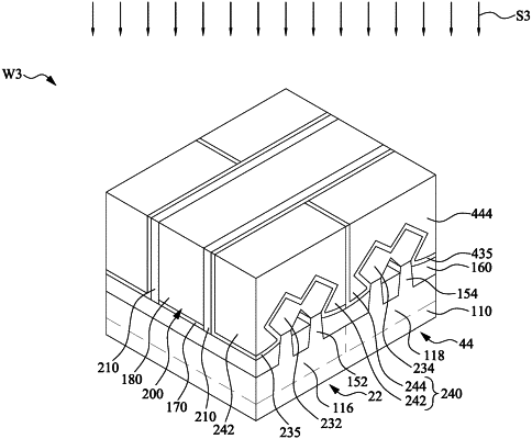
1. A semiconductor device, comprising:
an N-type fin-like field effect transistor comprising:
a first semiconductor fin;
a gate structure across the first semiconductor fin; and
a first source/drain feature in contact with the first semiconductor fin;
a P-type fin-like field effect transistor comprising:
a second semiconductor fin;
the gate structure across the second semiconductor fin; and
a second source/drain feature in contact with the second semiconductor fin;
a shallow trench isolation (STI) structure surrounding the first and second semiconductor fins;
a first interlayer dielectric (ILD) layer covering the first source/drain feature; and
a second ILD layer covering the second source/drain feature, wherein a porosity of the second ILD layer is greater than a porosity of the first ILD layer.
|