| CPC H01L 21/823481 (2013.01) [H01L 21/02356 (2013.01); H01L 21/76224 (2013.01); H01L 27/0886 (2013.01); H01L 21/022 (2013.01); H01L 21/0214 (2013.01); H01L 21/0217 (2013.01); H01L 21/02148 (2013.01); H01L 21/02164 (2013.01); H01L 21/02181 (2013.01); H01L 21/02183 (2013.01); H01L 21/02189 (2013.01); H01L 21/02192 (2013.01); H01L 21/02194 (2013.01); H01L 21/02271 (2013.01)] | 20 Claims |
|
1. A method for forming a semiconductor device structure, comprising:
forming a fin structure over a semiconductor substrate;
forming an isolation layer over the fin structure and the semiconductor substrate;
forming a protective layer over the isolation layer;
forming a dielectric layer over the protective layer; and
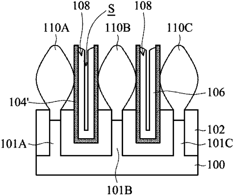
partially removing the isolation layer, the protective layer, and the dielectric layer, wherein a remaining portion of the isolation layer forms an isolation structure, remaining portions of the protective layer and the dielectric layer form a dielectric fin, the remaining portion of the protective layer forms a protective shell of the dielectric fin, the remaining portion of the dielectric layer forms a dielectric structure of the dielectric fin, the isolation structure laterally surrounds a lower portion of the fin structure and a lower portion of the dielectric fin, the protective shell has a first dielectric constant, the dielectric structure has a second dielectric constant, the first dielectric constant is higher than the second dielectric constant, the protective shell has a first average grain size, the dielectric structure has a second average grain size, and the first average grain size is larger than the second average grain size.
|