| CPC H01L 21/823481 (2013.01) [H01L 21/76224 (2013.01); H01L 21/823431 (2013.01); H01L 27/0886 (2013.01); H01L 29/0649 (2013.01); H01L 21/31053 (2013.01)] | 20 Claims |
|
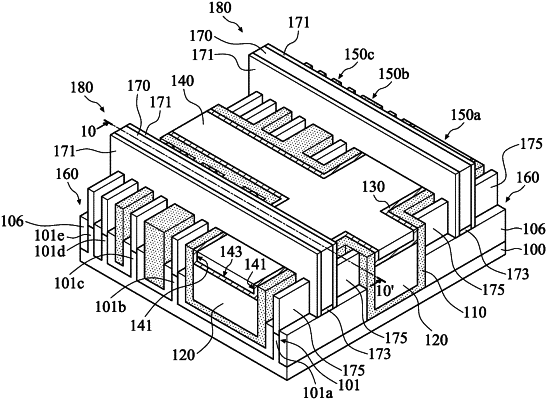
1. A semiconductor device structure, comprising:
a substrate having adjacent first and second fins protruding from the substrate;
a first gate structure and a second gate structure across the first and second fins, respectively;
an insulating structure between the first gate structure and the second gate structure, comprising:
a first insulating layer separating the first fin from the second fin;
a capping structure formed in the first insulating layer; and
a second insulating layer covered by the first insulating layer and the capping structure; and
a first insulating liner formed between the substrate and the first gate structure, and a second insulating liner formed between the substrate and the second gate structure, wherein the first insulating liner and the second are separated from each other by and in direct contact with the insulating structure.
|