US 11,688,633 B2
Passivation layer for integrated circuit structure and forming the same
Chun-Chiang Chen, Hsinchu (TW); Chun-Ting Wu, Kaohsiung (TW); Ching-Hou Su, Hsinchu (TW); and Chih-Pin Wang, Hsinchu (TW)
Assigned to TAIWAN SEMICONDUCTOR MANUFACTURING CO., LTD., Hsinchu (TW)
Filed by TAIWAN SEMICONDUCTOR MANUFACTURING CO., LTD., Hsinchu (TW)
Filed on Jul. 16, 2021, as Appl. No. 17/378,566.
Application 17/378,566 is a continuation of application No. 16/744,014, filed on Jan. 15, 2020, granted, now 11,069,562.
Prior Publication US 2021/0343587 A1, Nov. 4, 2021
Int. Cl. H01L 21/768 (2006.01); H01L 23/522 (2006.01); H01L 21/02 (2006.01); H01L 23/00 (2006.01)
CPC H01L 21/76832 (2013.01) [H01L 21/02274 (2013.01); H01L 21/76834 (2013.01); H01L 23/5226 (2013.01); H01L 24/11 (2013.01); H01L 24/13 (2013.01); H01L 2224/02381 (2013.01); H01L 2224/0401 (2013.01); H01L 2224/13024 (2013.01)] 20 Claims
OG exemplary drawing
 
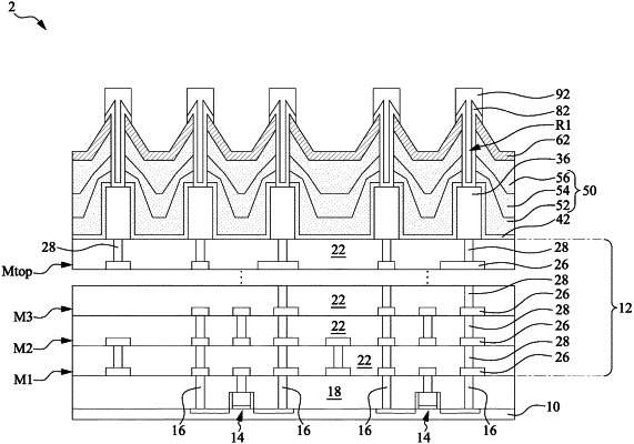
17. An integrated circuit (IC) structure, comprising:
a semiconductor substrate;
an interconnect structure over the semiconductor substrate;
a plurality of metal lines on the interconnect structure;
a porous liner over the plurality of metal lines;
a porous-free passivation layer over the porous liner; and
a nitride layer over the porous-free passivation layer.