| CPC H01L 21/76251 (2013.01) [B32B 3/02 (2013.01); B32B 18/00 (2013.01); H01L 21/02021 (2013.01); H01L 21/26506 (2013.01); H01L 29/04 (2013.01); H01L 29/0603 (2013.01); B32B 2250/02 (2013.01); B32B 2307/20 (2013.01)] | 15 Claims |
|
1. A method of manufacturing an epitaxy substrate, the method comprising:
providing a handle substrate;
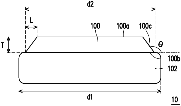
performing a beveling treatment on an edge of a device substrate such that a bevel is formed at the edge of the device substrate, wherein a thickness of the device substrate is greater than 100 μm and less than 200 μm;
performing an ion implantation process on a first surface of the device substrate to form an implantation region within the first surface; and
bonding a second surface of the device substrate to the handle substrate to form the epitaxy substrate, wherein a bonding angle greater than 90° is provided between the bevel of the device substrate and the handle substrate, and a projection length of the bevel toward the handle substrate is between 600 μm and 800 μm.
|