| CPC H01L 21/76224 (2013.01) [H01L 21/02532 (2013.01); H01L 21/22 (2013.01); H01L 21/3065 (2013.01); H01L 21/823431 (2013.01); H01L 21/823481 (2013.01); H01L 29/0649 (2013.01); H01L 29/0665 (2013.01); H01L 29/16 (2013.01); H01L 29/66545 (2013.01); H01L 29/66795 (2013.01); H01L 29/785 (2013.01)] | 9 Claims |
|
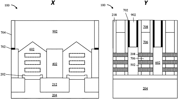
1. A semiconductor device comprising:
a nanosheet stack positioned over a substrate;
a dielectric pillar adjacent to the nanosheet stack, the dielectric pillar positioned on and in direct contact with a surface of a shallow trench isolation region of the substrate;
a source or drain (S/D) region on and in direct contact with the surface of the shallow trench isolation region such that a bottommost surface of the S/D region and a bottommost surface of the dielectric pillar are coplanar; and
a trench silicide on and in direct contact with a surface of the S/D region and on and in direct contact with a topmost surface of the dielectric pillar.
|